2013-2016


CARTOON


Small or medium-scale focused research project (STREP)
ICT FET Open Call
CARTOON FP7-ICT-2013-C
Starting date: Nov.1st, 2013
Partners
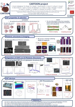
Université Paris Sud (coordination)
Technische Universität Dresden
Università degli Studi di Firenze
Commissariat à l’Energie Atomique et aux Energies Alternatives


Overview
Primary goal of the proposed research action is the development of a novel strategy for hybridizing silicon based photonic devices, exploiting semiconducting single-walled carbon nanotubes (s-SWNT) as integrated light source, modulator and detector. Photonics in Information and Communication Technologies (ICT) is more and more investigated for a broad application domain.
These applications require efficient optoelectronic devices to emit, modulate and detect light. To facilitate photonic and electronic convergence, the envisioned approach is based on the silicon platform. However, the definition of optoelectronic devices requires several kinds of materials (Si, Ge and III-V) as silicon is an indirect-gap material with poor electro-optic properties.
This project aims at investigating a new and innovative field through the use of SWNT in the near infrared (NIR) wavelength range. The main breakthrough will come from the development of SWNT-based optoelectronic components directly co-integrated within a silicon platform to address the major challenges of photonics. Such integration has never been investigated so far and thanks to a joint experimental and theoretical investigation our major goal is to establish the potential of SWNT technology for nanophotonics applications.
The project reposes on three major cornerstones:
-
(i)A waveguide detector in the 1.3-1.6µm wavelength range,
-
(ii)integrated optical modulators using Kerr (electro-refraction) and Stark (electro-absorption) effects and
-
(iii)An integrated electrically pumped optical nanosource. Each of these cornerstones will be a world's premiere and will constitute a breakthrough. Inherently, this makes it a high risk/high gain yet achievable proposal with a foundational impact both in knowledge and technology for nanophotonics. In a long term vision the establishment of new state of the art and advanced know-how on optoelectronic devices based on SWNT will allow developing and addressing a broad range of applications in information technologies.
CARbon nanoTube phOtONic devices on silicon

Meet us
On February 1st, 2017
in San Francisco
SPIE Photonics West
On December 8-10 2016
in Paris
NanoP conference